New Image Sensor
Feb 24 2021
Image sensor primarily converts photons into electrons.
Introduction of Cmos Sensor was a break through which enabled sensor size to manufactured to be bigger one.
Recent news Nikon developed a cutting edge technology of Image Sensor that controls light both dark and bright areas of image automatically.
Nikon is also engaged in research and development of cutting-edge image sensors, which are the core of video technology, based on optical technology, precision measurement / processing technology, and material technology. Currently, image sensors are used not only in the video field such as digital cameras and smartphones, but also in various industrial fields such as automobiles. In all fields, there is a demand for image sensors that achieve all of compactness, light weight, high frame rate, wide dynamic range, and high resolution.
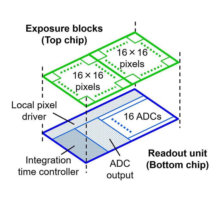
 This image sensor is constructed in a way it has two layers.
The top chip has 16 x 16 pixels as one block, and 264 x 264 blocks (4224 x 4224 pixels) are divided and arranged on one screen. It is possible to finely control the exposure time of these blocks from the bottom chip for each area on the screen.
With this function, you can express a wide dynamic range, and even for subjects with a large difference in brightness, you can clearly shoot the entire screen without crushing the dark areas or overexposing the bright areas.
Additionally this sensor can shoot 1000fps at 4k resolution with high dynamic range.
Manufacturing process
65 nm BSI + 65 nm CMOS stacking process
Image sensor1-inch CMOS image sensor
Pixel size 2.7 × 2.7 μm
frame rate1000 fpsDynamic range110 dB (at 1000 fps)
134 dB (at 60 fps)Total number of pixelsApproximately 17.84 million pixels (4224 x 4224 pixels).
Cameras made by this sensor yet to be announced.
CJ Rajkumar
Author/ Cinematographer